New Product Release | 4-Layer Laser Stacked Hole Storage Chip Packaging Substrate
- Release time: June 8, 2025
- Author: Founder
Recently, the company successfully delivered a 4-layer laser stacked hole storage chip packaging substrate. With three core technological breakthroughs in material innovation, heat dissipation design, and high-density interconnection, it provides high-performance packaging solutions for consumer electronics, data centers, AI computing power, and other fields, helping to promote the innovative development of the domestic storage chip industry.

Product size: 18mm × 7mm
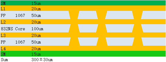
Finished board thickness: 0.3 ± 0.03mm
Surface treatment: ENEPIG (nickel palladium)
Assembly method: WB-BGA (wire bonded ball grid array package)
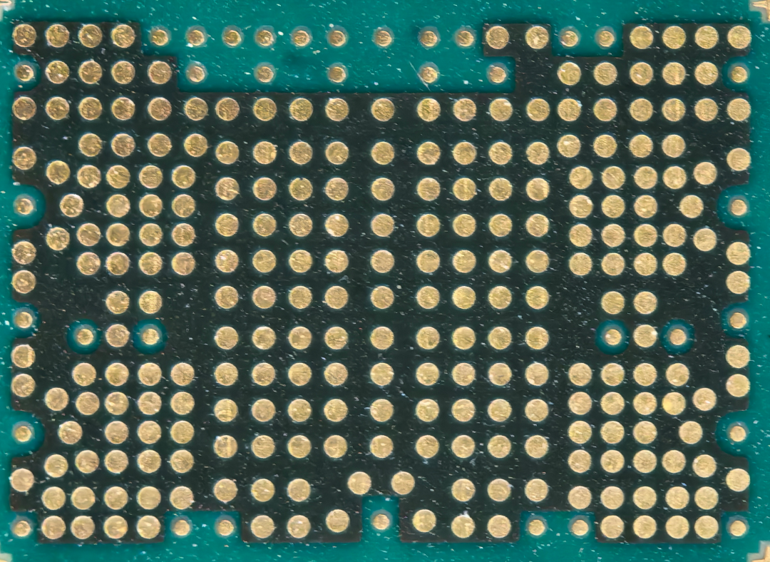
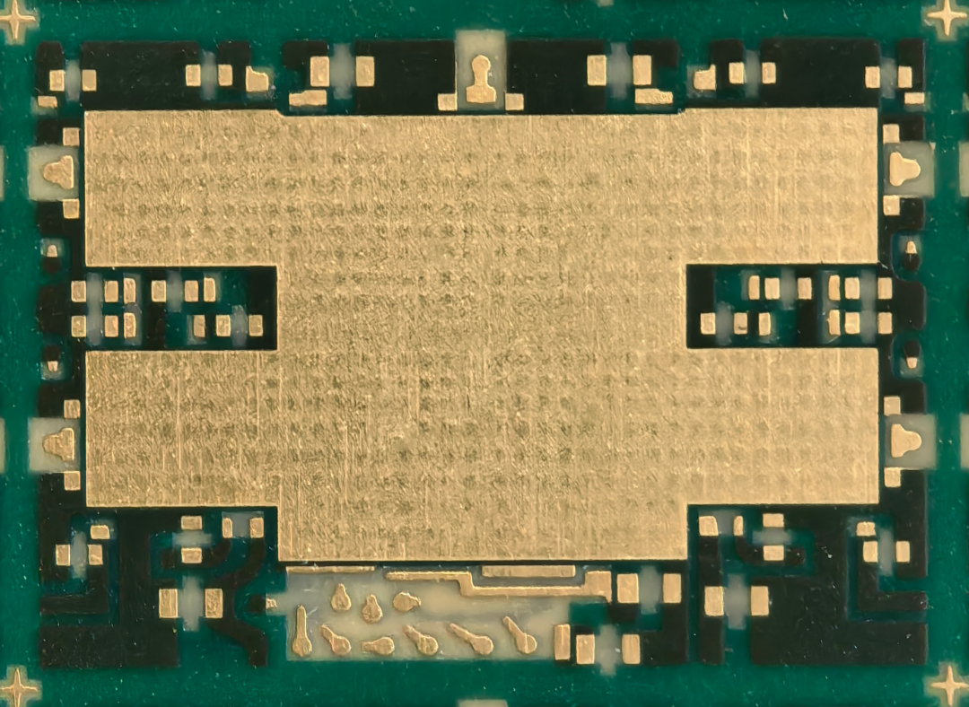
2. Product Display


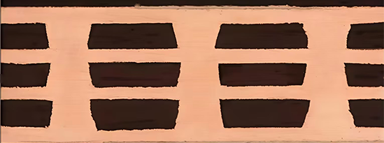
3. Stacked Display


Paired with Mitsubishi Gas 832NSF (LCA) series ultra-low CTE materials, the thermal expansion coefficient of the chip is highly consistent, significantly reducing temperature stress damage and ensuring stability in extreme environments.
通过创新结构提升30%散热效率,有效解决高负载场景下芯片过热导致的性能衰减问题,适用于AI服务器、数据中心等高功率设备。
4-layer blind buried hole wiring achieves a precision process with a line width/spacing of 30 μ m, supports high-speed data transmission, and meets the stringent requirements of signal integrity for the next generation of storage chips.
0.3mm轻薄化设计与高性能表现,可广泛应用于智能手机、可穿戴设备等消费电子领域,助力终端产品实现体积与性能的平衡;通过材料与散热优势,能为企业级存储系统及AI芯片提供稳定支撑。
