The first IC carrier board from Yingchuang Li has been shipped!
- Release time: May 4, 2024
- Author: Founder
Yingchuang Power
Start of innovative development strength
Carrier Board Division
The first IC carrier board has been shipped!!

IC Package Substrate is a carrier that connects and transmits signals between bare chips (DIEs) and printed circuit boards (PCBs), and is a key component in the packaging and testing process. It is developed based on the relevant technologies of PCB boards and is used to establish signal connections between ICs and PCBs, playing a role of "connecting the top and the bottom".
With the development of terminal electronic products towards multifunctionality, intelligence, and miniaturization, the demand for high integrated circuits has accelerated the rapid growth of the packaging carrier market. In the packaging carrier market, WB-BGA packaging type carriers have a huge market share, and packaging products are widely used in fields such as smartphones, smart homes, and smart wearables.

Product Introduction
Number of layers | 2nd floor |
surface handle | Soft gold+EB (electroplated soft gold+etched lead) |
finished product Plate thickness | 600 ± 50 μ M |
encapsulation way | WB-BGA |
application area | Livelihood consumption IC |
product characteristic | ① Minimum line width and spacing 40/40 μ m ② Minimum aperture of 150 μ m ③平整度≤8μm |
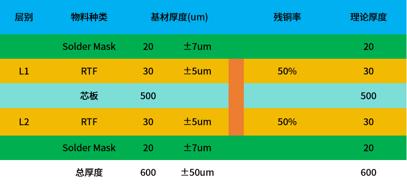
Layered design
Bind Gold Finger PAD
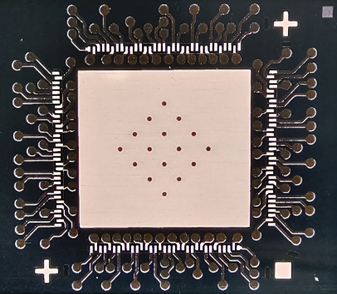
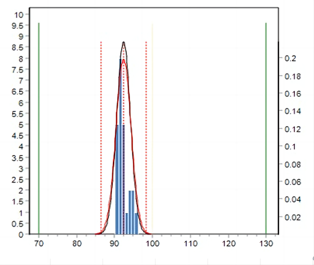
The center position is equipped with a large gold surface mounted chip, and the bottom heat dissipation is conducted through a through-hole.
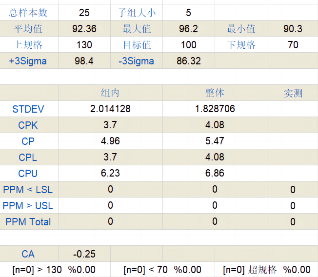
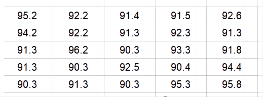
A row of 33 gold fingers for threading, totaling 132 gold fingers.
● 金手指宽度 CPK 4.08。
BGA pad width
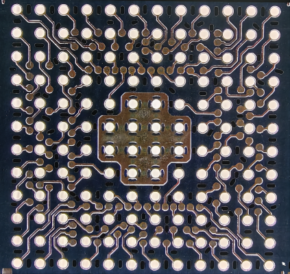
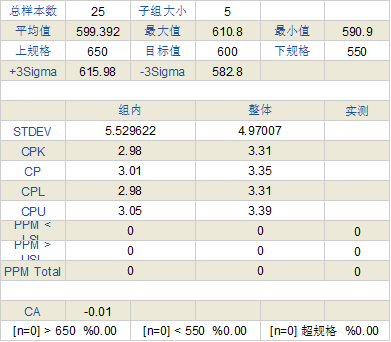
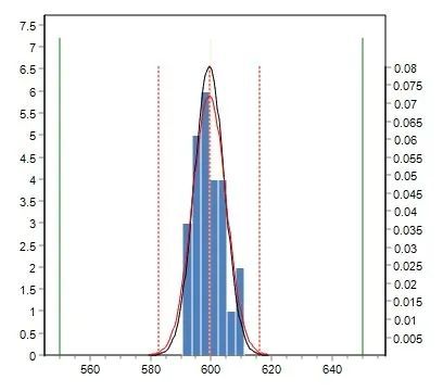

The center position is equipped with a large gold surface mounted chip, and the bottom heat dissipation is conducted through a through-hole.
A row of 12 solder ball pads, totaling 144 pads.
● 焊盘宽度 CPK 3.31。
pull test
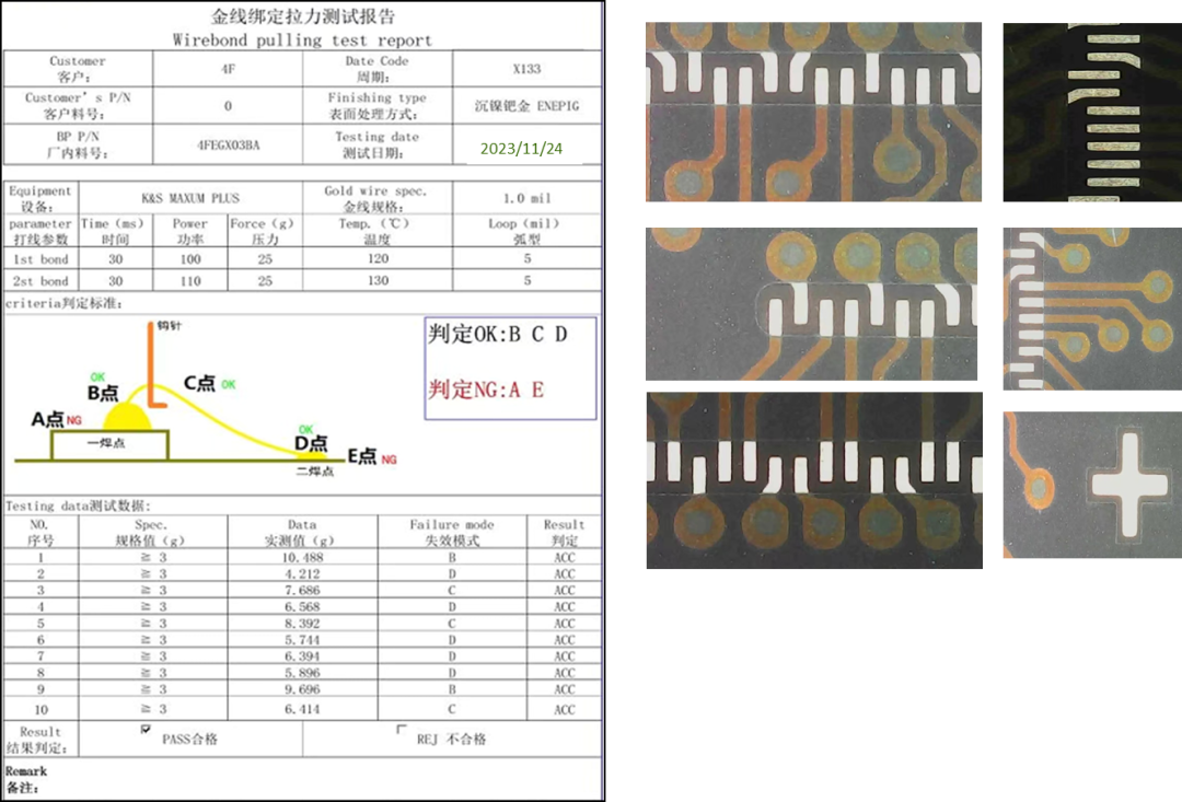
● 金线绑定拉力测试,判定ACC。
The minimum tensile force is greater than or equal to ≥ 3g, with a minimum tensile force of 4.212g.
● 光学十字标点,中心直角判读容易。
